
APPLICATIONS
DESIGN SUPPORT


Search
- Home
- Power ICs
- DrMOS + Smart Power Stages (SPS)
- AOZ5517MQI
AOZ5517MQI
DrMOS + Smart Power Stages (SPS)
Status: New
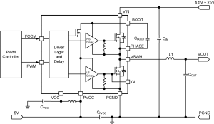
The AOZ5517MQI is a high efficiency synchronous buck power stage module consisting of two asymmetrical MOSFETs and an integrated driver. The MOSFETs are individually optimized for operation in the synchronous buck configuration. The High-Side MOSFET is optimized to achieve low capacitance and gate charge for fast switching with low duty cycle operation. The Low-Side MOSFET has ultra low ON resistance to minimize conduction loss. The compact 5mm x 5mm QFN package is optimally chosen and designed to minimize parasitic inductance for minimal EMI signature.
Parametrics
Status | New |
Power Stage Type | DrMOS |
Package | QFN5x5A-30L |
Min Vin (V) | 4.50 |
Max Vin (V) | 25 |
Abs Max Vin (V) | 30 |
Max DC I (A) | 60 |
Max Peak I (A) | 120 |
PWM Input (V) | 5 |
Tri-State Range (V) | 1.6 - 3.4 |
Max Frequency (MHz) | 2 |
Shutdown Control | FCCM = TS, PWM = TS |
Enable Diode Emulation Mode | FCCM = L |
Thermal Flag | No |
OCP (A) | No |
HSD | No |
Pre-OVP | No |
Features
- 4.5V to 25V power supply range
- 4.5V to 5.5V driver supply range
- 60A continuous output current
- Up to 80A with 10ms on pulse
- Up to 120A with 10µs on pulse - Up to 2MHz switching operation
- 5V PWM / Tri-State input compatible
- Under-Voltage LockOut protection
- FCCM pin control for Shutdown / Diode Emulation / CCM operation
- Standard 5mm x 5mm QFN-30L package
Documentation
| Title | Type | Date | File |
|---|---|---|---|
| AOZ5517MQI Datasheet | Datasheets | 2025-01-08 | |
| AOZ5517MQI Marking | Markings | 2025-01-08 | |
| AOZ5517MQI Reliability Report | Reliability Reports | 2025-01-08 | |
| QFN5x5A_30L_EP3_S | Package | 2023-04-05 | |
| QFN5x5A_30L_EP3_S Tape & Reel | Tape & Reel | 2023-04-05 |
Package Details
| Package Name | Dimensions | Package Specifications | Packaging Method |
|---|---|---|---|
| QFN5x5A_30L_EP3_S | 5.0x5.0x0.75 | Tape and Reel |